Professor Po-Tsun Liu’s Team at National Yang Ming Chiao Tung University Publishes Cutting-Edge Research on Heterogeneous Semiconductor Integration for Three-Dimensional Monolithic Complementary Field-Effect Transistors (CFETs) in 《Advanced Science》”
As Moore’s Law keeps advancing, the size of transistors is approaching the physical limit of miniaturization. Transistor structures have been evolving from traditional two-dimensional planar structures to three-dimensional device structures, such as Fin and Gate-All-Around FETs. In addition, the technology generation beyond Moore’s law has entered the era of integrating different functions, types, and even different kinds of heterogeneous semiconductor devices and circuits in a single-chip system within a limited footprint. The concept of three-dimensional integrated circuits (3D-ICs) has been proposed, which can be divided into Through Silicon Via (TSV) and Monolithic Three-dimensional Integration (M3D-IC) technologies. For the TSV process, the thinning of Si wafer thickness must be implemented, and the metal plugs of the silicon vias need to be defined by using high aspect ratio etching technology. These process steps are prone to cause a significant drop in product yield, which increases the technical cost of the product. In order to effectively solve the problems caused by the TSV technology, the monolithic-3D integration technology has been developed, as shown in Figure 1. M3D-IC technology refers to the implementation of additional transistor device layers by back-end-of-line (BEOL)-compatible processes above the front-end-of-line (FEOL) transistor layer to complete the multi-layer integrated circuit architecture. However, the major challenge of this technology requires the BEOL-compatible thermal budget (process temperatures lower than 500 degrees Celsius), and the resultant transistors must still maintain excellent electrical performance and reliability characteristics.
In the ” Angstrom Semiconductor Initiative” promoted by the National Science and Technology Council (NSTC), Prof. Po-Tsun Liu’s team from the Department of Photonics, National Yang Ming Chiao Tung University, has recently developed M-3D heterogeneous semiconductor complementary field-effect transistors (CFET) and successfully formed an inverter logic circuit with a high voltage gain, low power consumption, and high noise margins, as shown in Figure 2(a)-(c). In particular, the high voltage gain (152 V/V) is comparable to that of a complementary inverter composed of single-crystal silicon-based transistors, and the power consumption is much lower than that of silicon crystal devices. The heterogeneous semiconductor device architecture is a vertically-stacked 3D structure in which a p-channel polycrystalline silicon thin-film transistor (poly-Si TFT) is used as the first transistor layer, and then an n-channel amorphous indium tungsten oxide thin-film transistor (a-IWO TFT) is stacked on top of it for M3D-IC applications. It can effectively increase the chip density. Furthermore, the a-IWO TFT with a channel thickness of only a few atomic layers can maintain excellent electrical performance, which is similar to 2D materials in terms of the current transport mechanism. The atomically thin oxide semiconductor channel can significantly suppress the leakage path and short-channel effect (SCE) of field-effect transistors so that the device can exhibit excellent performance even when it enters the short-channel scale. The outstanding results of the execution of this research project have been published in the internationally recognized journal “Advanced Science” (Heterogeneous Integration of Atomically-Thin Indium Tungsten Oxide Transistors for Low-Power 3D Monolithic Complementary Inverter, p. 2205481, Jan. 2023. IF: 17.52, FWCI: 3.32). The research results have extremely high technical value for the application of next-generation angstrom-level M3D-IC technology, which can realize heterogeneous integration with ultra-high chip density and high energy efficiency. It will be the continuation of “Moore’s Law” and the next important indicator leading the development direction of semiconductor technology.
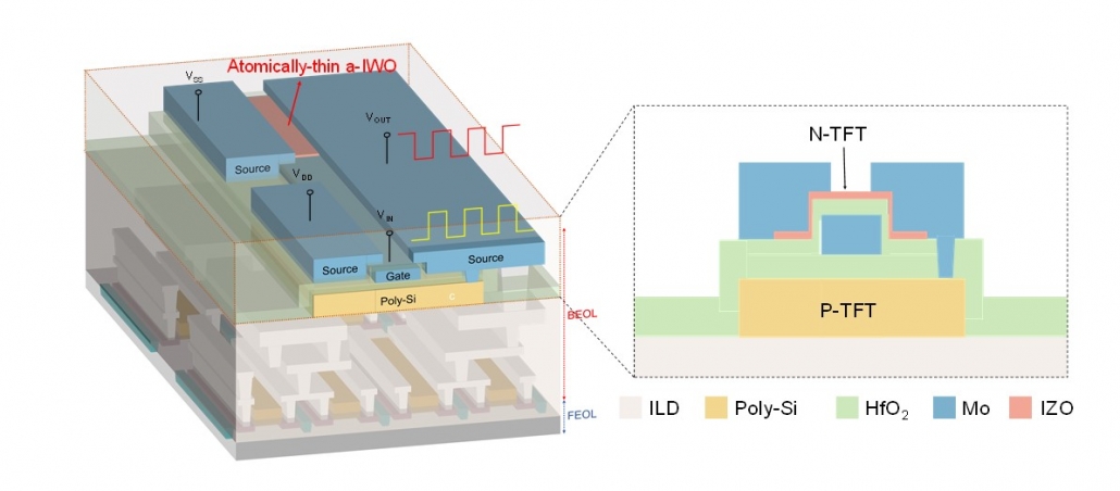
Figure 1| Vertical stacked heterogeneous complementary field-effect transistors (CFET), and interconnected to form an inverter for three-dimensional integrated circuits application.
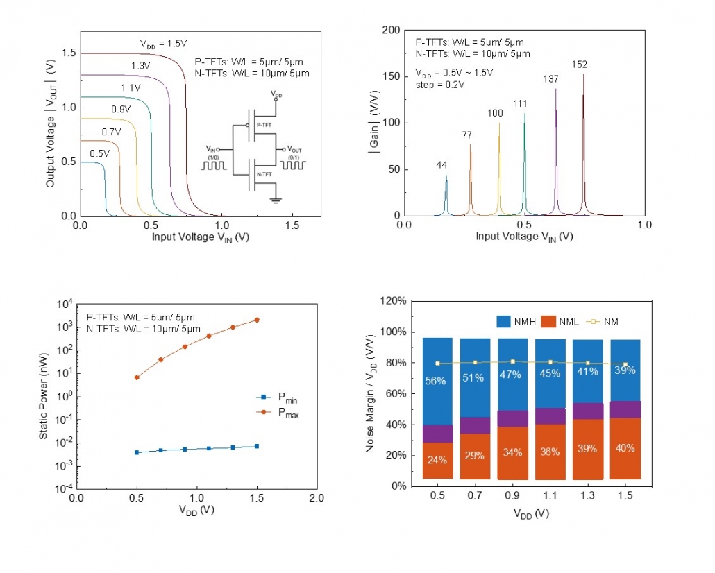
Figure 2| An Inverter comprised by CFETs, showing (a) voltage conversion curve, (b) voltage gain, (c) static power dissipation, and (d) noise tolerance at different operating bias voltages.