Project
Development of High-Density 3D Via-RRAM Device and Array in Advanced Technology
PI
Co-PI
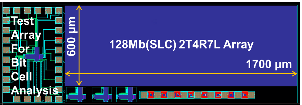
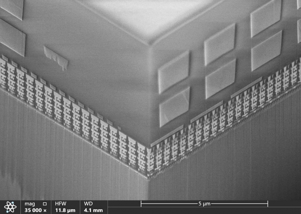
In 16nm technology node, a memory density of 0.13 Gb/mm2 for a 128Mb array has been achieved using a 3D Via RRAM 2T4XR device stacked with 7 metal layers. This embedded non-volatile memory technolgy is fully compatible with the CMOS FinFET logic process.
Through electrical analysis, the characteristics of 3D stackable with a total of 8 layers are verified. The memory cells utilize FinFET to control resistive switching operations and exhibit sufficient read windows. Moreover, by employing current-limiting operations, the Via RRAM demonstrates the ability for multi-level cell (MLC)operation, thus further enhancing memory density.

Fig. 1 SEM image of 7-layer 2T4XR 3D Via RRAM array, and the TEM image of X & Y cross-section.

Fig. 2 The floorplan of the 128Mb array in 2022Q4 tape-out
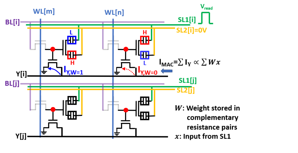
The innovative dual-bit latch-based in-memory-computing device combines high-density resistive memory with the concept of “latch” from digital logic gates. Implemented in a nano-scale CMOS front-end logic process, these gates store complementary non-volatile data in the dual-bit HKMG RRAM pairs, where data can be written and cleared within 40 ns, and data readout can be completed within 5 ns, effectively reducing energy consumption by 43%. Storing data directly within the component allows for logical operations, utilizing the amplification characteristics of an output transistor to significantly enhance the read window and achieve an over 800x increase in the On/Off ratio. The device also demonstrates multi-level cell (MLC) capabilities, for applications in analog multiplication-accumulation operations in neuromorphic computing chips, enabling high-density synaptic weight storage.

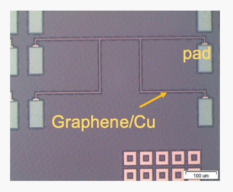
In the project, we propose a graphene synthesis strategy at 400°C throughout the process via chemical vapor deposition and plasma-assisted fabrication process. By adjusting parameters such as gas flow, growth temperature, and plasma energy, the thickness, quality, and electrical properties of graphene can be precisely controlled. The graphene growth technology on 0.4~10 μm-width copper wires with the 16 nm technology node has been verified. Based on the Raman spectrum measured results, the material on the copper wire is confirmed to be graphene, and the quality of graphene grown under different parameters is analyzed. Additionally, it has been demonstrated that the conductivity of graphene/copper hybrid interconnects is higher than that of pure copper, offering great potential for high-performance circuits in the future.


