Project
Technology development of key materials and devices for sub- nanometer 2D field-effect transistors
PI
Co-PI
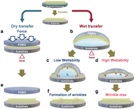
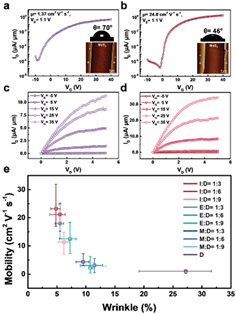
This project focuses on the growth of large-area two-dimensional thin films and the development of high-quality transfer techniques. The team has successfully developed a high-quality two-dimensional material transfer technique, and the related findings were published on “Advanced Functional Materials” (IF: 19.9) under the title: “Rational design on wrinkle-less transfer of transition metal dichalcogenide monolayer by adjustable wettability-assisted transfer method.”
In this research, an adjustable wettability-assisted transfer method was developed, utilizing different transfer medium mixtures to reduce the density of wrinkles and achieve high-quality transfer of two-dimensional materials, improving the intrinsic electrical performance of two-dimensional channel materials. By controlling the wettability of the transfer medium with different proportions of alcohol and deionized water, the transition metal dichalcogenide (TMDC) monolayer was successfully adhered to the target substrate, thus achieving wrinkle-less transfer of the TMDC monolayer. Using this method, the wrinkle density was reduced by 15 – 20% compared to traditional pure deionized water transfer methods. Transferring MoS2 monolayers using the alcohol-water mixture resulted in an enhanced carrier mobility (20-35 cm2V-1s-1), which is 30 times higher than the carrier mobility achieved through pure water transfer.
This research provides solid technical support for the development of transfer techniques for large-area two-dimensional thin film materials. In subsequent projects, this method was successfully used to achieve the high-quality transfer of large-area two-dimensional channel materials.
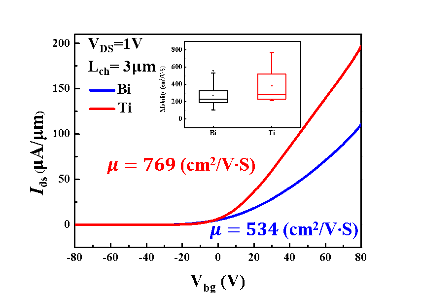
In Subproject 2, we investigated the contact characteristics and interface cleaning techniques of two metals, Bi and Ti, on the channel material Bi2O2Se. Our goal was to fabricate a back-gate field-effect transistor (FET) based on Bi2O2Se with the highest room-temperature electron mobility reaching 769 (cm2/V·S). To account for the potential influence of varying Bi2O2Se channel thickness, we created a control group using identical processing parameters. Comparing the FETs produced, those with Ti contacts exhibited significantly higher drive currents and electron mobilities compared to the FETs utilizing the semimetal Bi, with a difference of nearly 2 times in drive current. These results clearly demonstrated the superior contact characteristics of Ti. Subsequent statistical analysis further confirmed Ti as the optimal contact metal for high-performance field-effect transistors, achieving a maximum drive current of 2 × 10⁻⁴ (A/µm) and an extremely high current on-off ratio of 109, showcasing exceptional device performance.
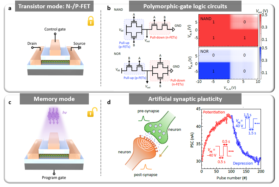
Reconfigurable field-effect transistors (RFET) are recognized as a potential candidate for next-generation electronics. Simplifying the complexity of electronic fabrication is its primary benefit, but the huge power consumption becomes a critical defect because of the need of an external electrostatic field for fine-grain reconfiguration at runtime. Here, we propose an all-2D photo-trapping RFET based on h-BN/2D channel/h-BN heterostructure on a SiO2/Si substrate, which endows non-volatile and dynamically tunable polarity. Through transistor-mode operation in our prototype devices, circuit functionalities of basic logic circuits have been demonstrated. In its memory-mode operation, synaptic functions of biological features are shown for neuromorphic computing.
Our team focuses on the development and validation of two-dimensional (2D) material transistors for integrated circuit applications, leveraging semiconductor process-compatible technologies. The key achievements include:
- Development of an integratable top-gate transistor: We have successfully applied a dual-layer gate dielectric technique to realize a back-end-of-line (BEOL) WS2 top-gate transistor with an ultra-low threshold swing (80mV/dec) with CVD growth temperatures less than 300°C. The device characteristics and structure are comparable to existing silicon base FET and meet the standards of leading international teams specializing in 2D material transistors.
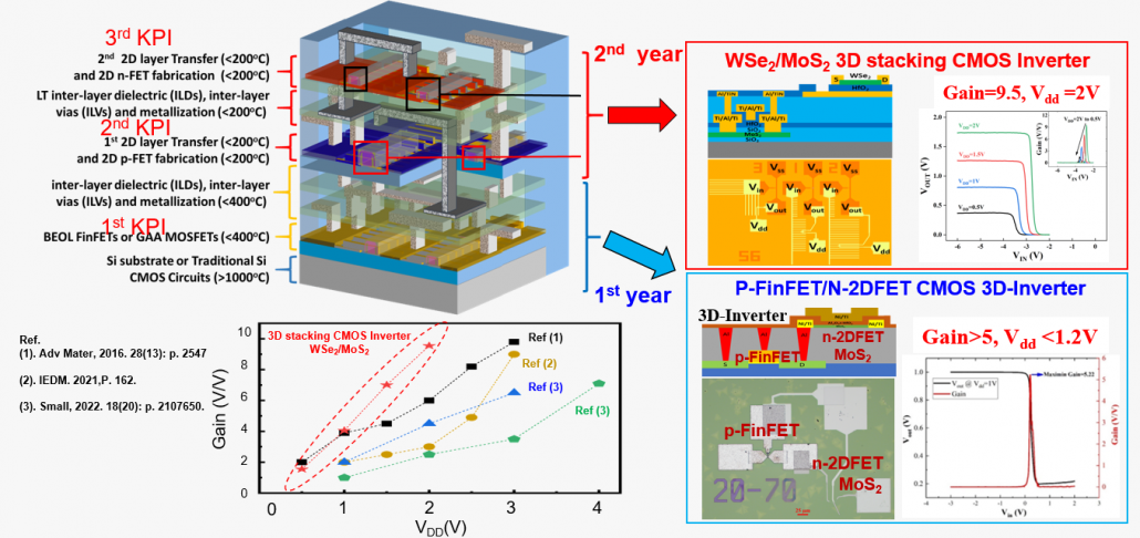
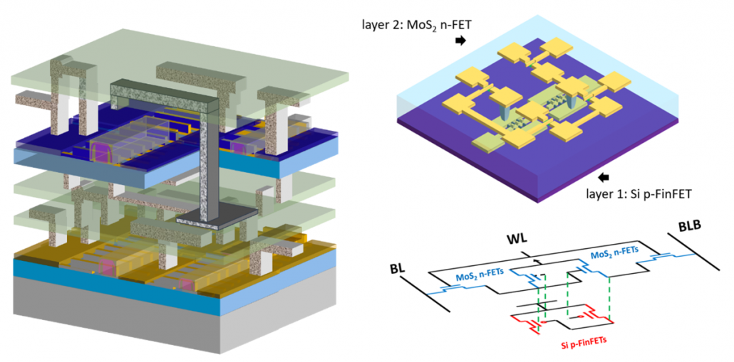
- 2. Monolithic 3D Si p-FinFETs/2D n-MOSFETs CMOS inverter: The distance between the top and bottom device layers is just 400nm. The monolithic 3D CMOS inverter demonstrates excellent characteristics with a supply voltage (Vdd) of less than 1V and a gain greater than 5. This verifies that high-performance, high-density monolithic three-dimensional integrated circuits can be fabricated with 2D material transistors and mainstream silicon FinFET.
- All 2D material monolithic 3D CMOS inverter: By employing several low-thermal-budget techniques, we have successfully achieved three-dimensional vertical integration of top and bottom layers of p-type and n-type 2D material transistors. This demonstrates the feasibility of monolithic 3D integrated circuits using all 2D material transistors. The all 2D material monolithic 3D CMOS inverter displays superior characteristics with a supply voltage (Vdd) of less than 2V and a gain greater than 9.
