Project
3D Embedded Memory Architecture of Resistive-gate NVM:
Implementation of NOR and NAND
PI
Co-PI
Collaborator
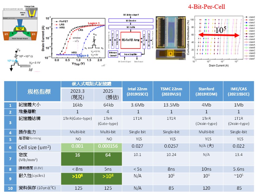
QLC(Quad Levek Cell)- The world first 4-bit/cell Resistance Memory
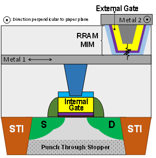
In phase 2 we have setup an efficient FinFET platform which was then integrated with MIM to demonstrate an 1kbit RRAM chip. Owing to its unique gate-type 1T1R architecture, it is superior to the conventional drain-type architecture used in the industry and academia, and is feasible for 3D development. The demonstration is a heterogeneous integration of 1kb array that we made at TSRI and peripheral circuits via tsmc shuttle. Also, through the design of 1T16R architecture, a density of 16x, i.e., 16kbits can be accomplished. Overall, the proto-type has salient features: (1) small cell size in which a unit cell has multi-bit capability, e.g., 4-bit-pre-cell, (2) a very wide range of window up to (2×10⁵) while the other reported had 10-100x window at most, (3) more than 108 endurance, and (4) decade-lifetime can operate up to 1250C to maintain excellent retention, better than Intel and tsmc’s RRAM in production so far.
References: 1. M. Y. Lee, J. P. Wu, C. H. Liu, J. C. Guo, and S. S. Chung, “A World First QLC RRAM: Highly Reliable Resistive-Gate Flash with Record 108 Endurance and Excellent Retention,” in IEEE IRPS, March 27-30, 2023.
2. E. R. Hsieh, K. T. Chen, P. Y. Chen, S. Wong, S. S. Chung, “A FORMing-Free HfO2/HfON-Based Resistive-Gate Metal–Oxide–Semiconductor Field-Effect-Transistor (RG-MOSFET) Nonvolatile Memory With 3-Bit-Per-Cell Storage Capability,” in IEEE Transactions on Electron Devices, vol. 68, no. 6, pp. 2699-2704, June 2021.

Design Guidelines of 3nm FinFET
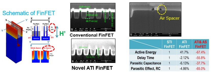
Following our effort in recent years, we have established a 3nm FinFET device fabrication capacity. In this design, we used a novel ATI(Active Trench Isolation) method to enlarge the width extending toward the substrate such that Ion current enhancement can be achieved with the same foot-print. Also, by using the air-spacer, a factor of 1.43 in speed and 54% of power reduction can be achieved. This provides a stable FinFET process and can be readily for users of the industry. Also, it serves as a major platform for our development of Resistance memory.
Reference: (Invited) S. S. Chung, et al., “The Extension of the FinFET Generation Towards Sub-3nm: The Strategy and Guidelines,” IEEE EDTM, March 5-9, Oita, Japan, 2022)

A Physical Unclonable Function Implemented in FinFET-based Resistance Memory
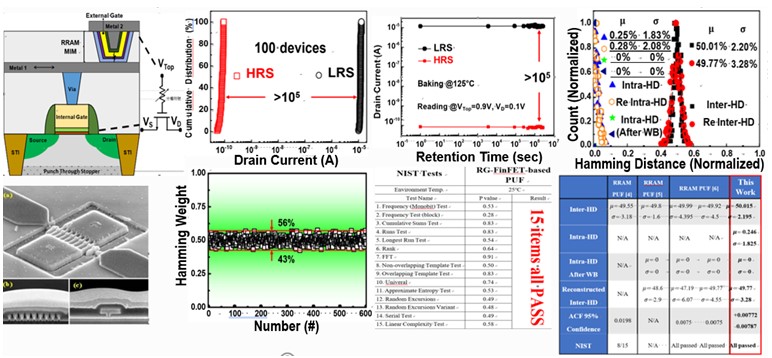
A paper entitled “The Demonstration of a Physical Unclonable Function (PUF) on a Resistive-Gate FinFET Memory “, by the team was published in 2022 Japan largest semiconductor conference, SSDM. It exhibits a 1kbit RRAM with features of PUF. This paper was listed as candidate of SSDM best paper award. In this study, a 1kb FinFET-based resistance was first built and then an excellent security measures were examined, including Intra-HD, Inter-HD, HW, Auto-correlation, NIST-Test etc.
Reference: M. Y. Lee, T. J. Kao, Y. C. Lee, E. R. Hsieh, J. C. Guo, and S. S. Chung, “The Demonstration of a Physical Unclonable Function (PUF) on a Resistive-Gate FinFET Memory,” SSDM, pp. 449-450, Chiba, Japan, 2022.


