Project
Low-dimensional Materials on Advanced and High Performance
Electronics Integration
PI
Co-PI
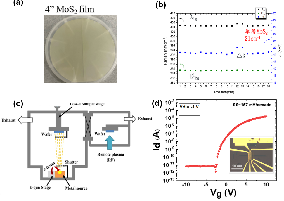
Our team has successfully developed a large-area and low-temperature synthesis process and equipment for MoS2 growth. This technology enables the growth of single-layer MoS2 on wafer-scale substrates (4″) at temperatures below 550°C. This achievement has been transferred to a semiconductor company in Taiwan. Moreover, we have established a unique platform that enables atomic-level manipulation for interface modification of two-dimensional materials, effectively improving device performance.
Furthermore, this technology has been granted 1 patent in Taiwan and is currently under review for 3 patent applications in the United States.

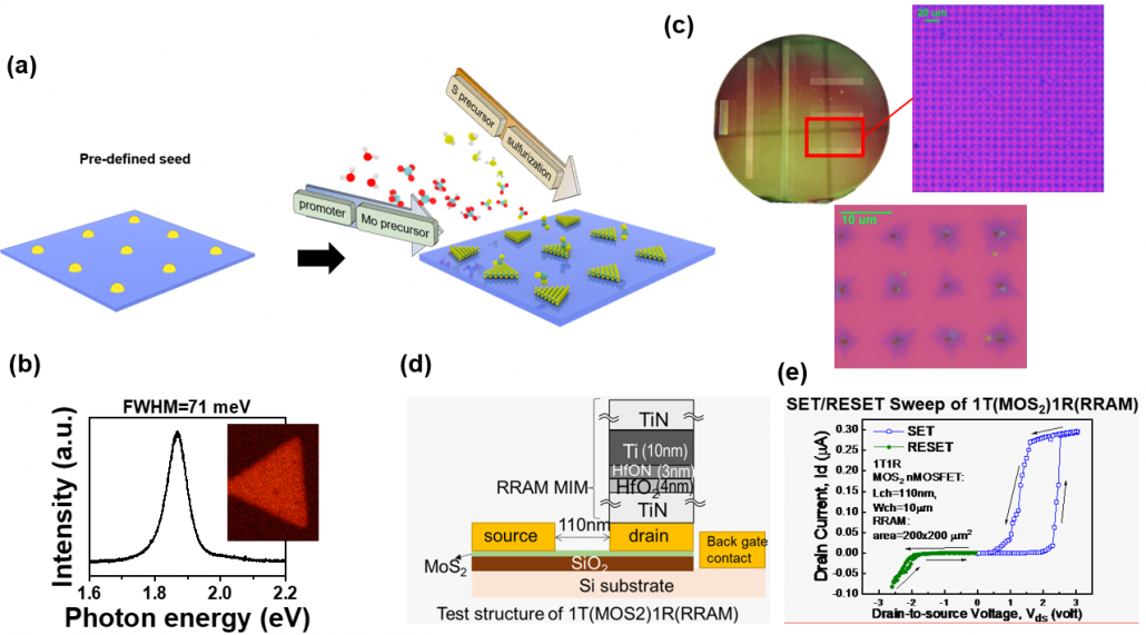
Our team has developed a BEOL-compatible growth technology that can be directly applied to device processes. This technology utilizes novel precursors combined with promoting agents and incorporates a pre-defined seeding substrate design. Moreover, for the first time, we demonstrate the real BEOL process that enables single-crystal growth at low temperatures (400℃) directly on SiO2 oxide substrates. Subsequently, we showcase the integration of lower-power and forming-free 1T-1R RRAM devices. These devices demonstrate excellent stability, with a voltage below 3 V, PGM_Current less than 1 μA/μm, endurance exceeding 106 cycles, and a retention period of 10 years at 100°C. The achievement was presented at the 2D-TMD 2023 conference.

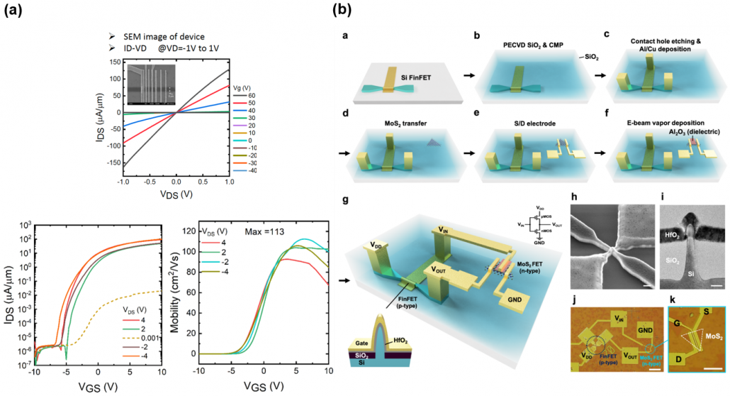
Our team has conducted metal selection and optimization to effectively achieving contact resistance down to 95 ohm·μm. The device also demonstrates a high on-current density of 90 μA/μm (VDS=1), indicating efficient carrier injection. The electron mobility achieved is 113 cm²/Vs, indicating good electron transport characteristics.
Furthermore, our team has proposed a stacked three-dimensional integration process technology for 2D materials and semiconductor devices. This technology involves integrating a high-mobility, high-drive-current P-type Si-based FinFET in the front-end with a low-temperature n-type MoS2 FET in the back-end to fabricate functional logic circuits that meet the requirements of back-end integration processes. The on/off current ratio and the on-current of both transistors show similar levels, implying a compatible performance as needed for CMOS implementation. The maximum voltage gain of ~38 is achieved. This significant achievement has been published in npj 2D Materials and Applications 7, 9 (2023).


