Project
Non-Si Atomic Layer Channel Materials: Single-crystal growth and device technology developments
- Team Members
PI
Prof. Wen-Hao Chang, Professor
Dept. Electrophysics, National Yang Ming Chiao Tung University
Co-PI
Prof. Horng-Chih Lin, Professor
Institute of Electronics, National Yang Ming Chiao Tung University
Prof. Chiung-Yuan (Gene) Lin, Associate Professor
Institute of Electronics, National Yang Ming Chiao Tung University
Prof. Chang-Hsiao Chen, Assistant Professor
Dept. Electrical Engineering, National Sun Yat-Sen University
- Introduction
This proposal aims at developing critical device technologies based on establishing the material synthesis technology of novel low-dimensional semiconductors. Two-dimensional (2D) materials hold great promises for surmounting the fundamental limits of conventional semiconductors and device frameworks, offering an unprecedented opportunity for the development of next-generation semiconductor technologies. To overcome the bottlenecks of 2D materials for practical device applications, this project synergizes a research team with interdisciplinary expertise of 2D materials and devices, proposing the integrated project entitled “Non-Si Atomic Layer Channel Materials: Single-crystal growth and device technology developments”. This proposal consists of five subprojects. Subproject #1 aims at developing the epitaxial growth technologies for large-area single-crystal 2D semiconductors by chemical vapor deposition (CVD). This subproject will focus on the four typical 2D semiconductors: MoS2, MoSe2, WS2 and WSe2 to achieve low defect density and high carrier mobility. For large-area (wafer-scale) growth technology, short-term goal is to achieve single-crystal growth on 2-inch wafers as a proof-of-concept demonstration, while the midterm and long-term goal of expanding the growth area larger than 4 inch will be achieved through collaboration with TIRI (Taiwan Instrument Research Institute). Subproject #2 proposes to established a CVD system in an ultra-clean and highly purified gas environment (low H2O and O2 concentration) to explore the growth techniques for new materials with high mobility other than the four typical 2D semiconductors, such as monochalcogenides and group-IV-element 2D materials. Subproject #3 is going to establish wafer-scale transfer techniques to realize noninvasive and ultraclean 2D materials after transfer processes. Subproject #4 will explore the strategy to achieve a low metal contact resistance based on first-principle calculations and non-equilibrium Green function theory for various metal contact configurations, which will provide a guidance for experimental realization of low contact resistance. Subproject #5 will develop novel fabrication processes for short-channel devices based on 2D materials, which can form a convenient and efficient device fabrication platform to characterize and verify the usefulness of the material growth, transfer processes and metal contacts developed by other subprojects for the ultimate device performance.

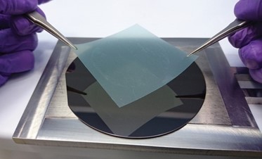
2-inch wafer scale single-crystal monolayer hBN transferred on 4-inch Si wafer.
- Phase I - Achievements
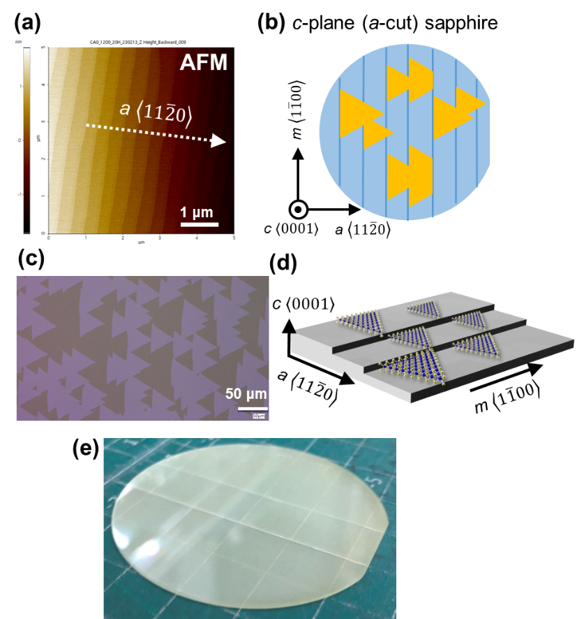
By surface engineering, surface atomic steps can be formed on sapphire substrate (a,b). Using CVD growth, single-oriented MoS2 grains can be grown of on these atomic steps (c,d). Continuing the growth, the MoS2 grains can be stitched into a single-crystal continuous film up to 2-inch wafer size.

A世代前瞻半導體技術專案計畫|ANGSTROM SEMICONDUCTOR INITIATIVE
*國科會計畫補助
Address|Program Office of Thrust 1&2
R313, Engineering Building D, 1001 University Rd., Hsinchu City 300, Taiwan
Address|Program Office of Thrust 3
RA201, Department of Physics, 88, Sec.4, Ting-Chou Rd., Taipei 116, Taiwan
