Project
Nanosheet extensions and beyond
PI
Co-PI
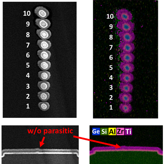
To further improve the performance of highly stacked GeSi channels, the 6 stacked GeSi nanowires without parasitic channel are demonstrated by optimizing the wet etching. The device has the SS of 80mV/dec and ION/IOFF of 1.5E5. The ION per stack of 120μA and ION per footprint of 4600μA/μm are achieved at VOV=VDS=0.5V among Ge/GeSi 3D nFETs. The results have been published in 2022 VLSI-TSA, and won the Best Student Paper Award. Increasing the number of stacked channels is needed to further enhance the transistor ION. The 10 stacked GeSi nanowires without parasitic channel are demonstrated with the ION per stack of 140μA (6500μA/μm), and the results have been published in 2022 SISC. The 16 stacked GeSi nanowires are demonstrated with the ION per stack of 190μA (9400μA/μm) by the co-optimization of CVD epitaxy and isotropic wet etching, and the results have been submitted to Nature communications engineering.

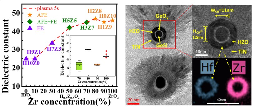
The systematic work to pursue high-κ dielectrics is presented by optimizing the [Zr] in HfxZryO2 in our work. The peak high κ value of 47 is achieved in Hf0.2Zr0.8O2. The high-κ Hf0.2Zr0.8O2 gate dielectric is integrated into the stacked Ge0.98Si0.02 nanowire nFETs. High ION = 67 μA per stack and ION per perimeter = 740 μA/μm at VOV = VDS = 0.5V are achieved with 450 oC PMA. The result of this work has been published on IEEE EDL, 2022.

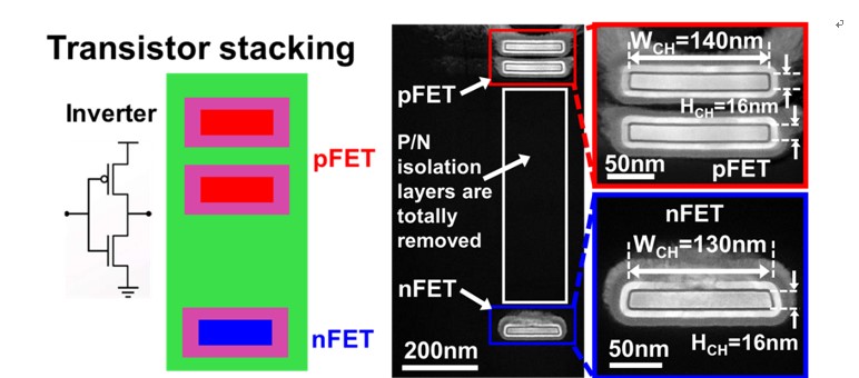
The pFET and nFET are able to fold on each other vertically to reduce 50% of cell area ideally in complementary FETs (CFET), as a promising transistor architecture beyond stacked nanosheets. The CFET transistor structure with 3D transistor stacking can enable further cell height scaling and Moore’s law scaling for 0.5nm technology node and beyond. Furthermore, high mobility GeSi channel is used for both nFET and pFET in CFET structure, while the process without S/D selective epitaxial growth can achieve self-aligned CFETs by multiple P/N junction isolation to effectively reduce the leakage current to replace dielectric layer isolation. The post-metallization annealing (PMA) with the low thermal budget of 400oC improves the inverter characteristics such as switching threshold voltage and voltage gain. The VTC of the Ge0.75Si0.25 CFET with a maximum gain of 9.6V/V at VCC=1.2V is achieved after the 400oC PMA. The results of GeSi CFET have been published in 2022 IEEE International Electron Devices Meeting.


