Project
Development for Advanced High-Density Monolithic Three Dimensional Integrated Circuits with Multi-stacked Transistor Layers (II)
PI
Co-PI
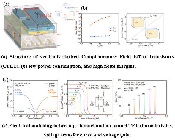
Prof. Po-Tsun Liu’s research team has successfully developed vertically-stacked Complementary Field Effect Transistors (CFETs) suitable for three-dimensional integrated circuits on a single chip. The performance of CFETs has been validated using an inverter circuit. This remarkable research achievement has been published in the prestigious academic journal “Advanced Science” under the title: “Heterogeneous Integration of Atomically-Thin Indium Tungsten Oxide Transistors for Low-Power Three-Dimensional Monolithic Complementary Inverter“, p. 2205481, Jan., 2023. (Impact Factor: 17.52, FWCI: 3.32).
The inverters realized in this study exhibit high voltage gain, low power consumption, and high noise margins. The voltage transfer characteristics (VTC) of the inverter circuit demonstrate excellent matching between p-channel and n-channel TFT characteristics. Particularly, the output voltage gain can reach up to 152V/V, comparable to traditional silicon-based complementary inverters. The use of atomically-thin indium tungsten oxide films in the CFETs helps effectively suppress leakage current paths during device off-state, resulting in minimal static power consumption, as low as a few pico-watts, which is significantly lower than silicon-based devices. This groundbreaking research contribution is expected to propel the semiconductor industry into the next generation.

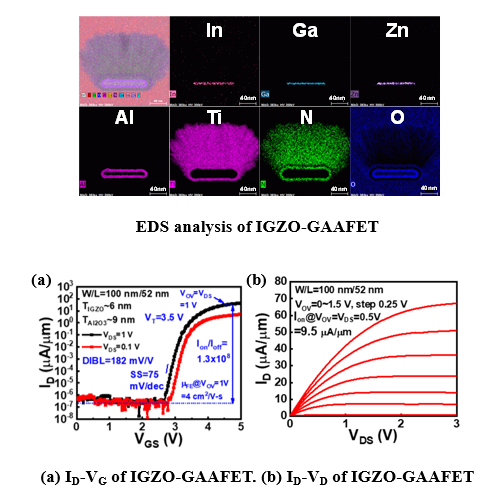
In this project, the first amorphous InGaZnO (a-IGZO) gate-all-around (GAA) nanosheet FET has been demonstrated at 2023 VLSI Symposium. All of the process temperatures are below 300℃, showing great back-end-of-line (BEOL) compatibility. The device with gate length (L) of 52nm shows Ioff <10-7 μA/μm (detection limit), high Ion/Ioff >1.3×10⁸, the enhancement mode with the positive threshold voltage (VT) of 3.5V. Moreover, the smallest SS of 61 mV/dec. among all oxide semiconductor nanowire/nanosheet devices is achieved.

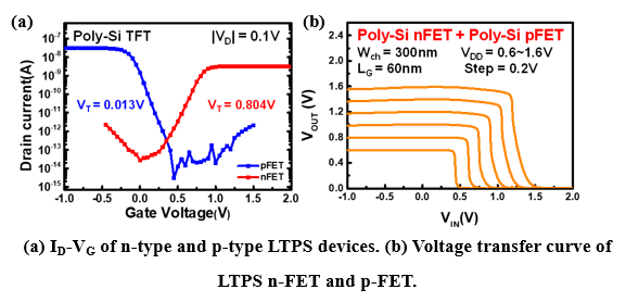
In this work, we have successfully developed BEOL compatible low thermal budget poly-Si FET for high density heterogeneous devices integration. By utilizing low-temperature PECVD to deposit amorphous Si, the process temperature can be controlled under 300℃. Furthermore, the green laser crystallization and dopant activation with varying inter-layer thickness were also investigated. To sum up, we have successfully developed n-channel and p-channel PECVD Poly-Si field-effect devices, followed by the integration of these two types of devices. This integration has exhibited good voltage transfer characteristics (VTC) of an inverter circuit, validating the feasibility of future heterogeneous semiconductor integration applicable for the advanced IC technologies.


