Project
- Introduction
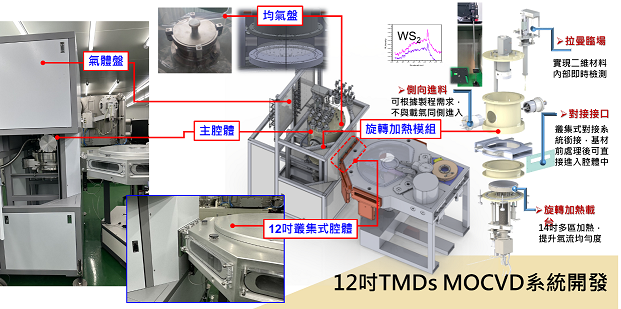
The main goal of this project is to develop the growth equipment and techniques of large-scale 2D materials for novel 2D semiconductor materials and next-generation device technology. Large-scale 2D materials fabrication and device verification platform will be delivered for early researches and developments of industry and academic groups. This platform will play a role like fundamental research core-instrument for 2D materials and open for industry and academicrese arch of advanced materials and devices. Finally, the experience and research results of this project could assist and upgrade the capabilities the domestic semiconductor equipment industry to access high added-value semiconductor equipment supply chain and lay out the next generation semiconductor fabrication market.

The main goal of this project is to develop the growth equipment and techniques of large-scale 2D materials for novel 2D semiconductor materials and next-generation device technology, and based on the spirit of the service platform, will provide industry-university-institute community to conduct prospective material research and development.
- Phase I - Achievements
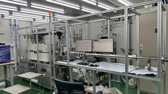
Gas-source Hot-wall MOCVD system

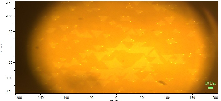
Growth of WS2 crystals with H2S source

A世代前瞻半導體技術專案計畫|ANGSTROM SEMICONDUCTOR INITIATIVE
*國科會計畫補助
Address|Program Office of Thrust 1&2
R313, Engineering Building D, 1001 University Rd., Hsinchu City 300, Taiwan
Address|Program Office of Thrust 3
RA201, Department of Physics, 88, Sec.4, Ting-Chou Rd., Taipei 116, Taiwan
