Project
Develop 3D dimensional/chemical metrology at a sub-nanometer
resolution for the next-generation semiconductor industry
PI
Co-PI
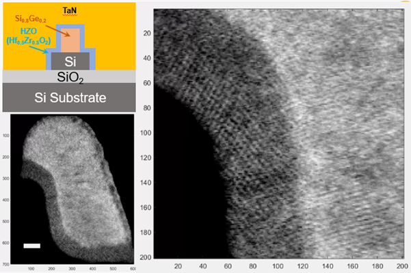
We use focused ion beams to prepare finFET needle-shaped samples, combined with STEM-Tomography technology to obtain an atomic resolution (1.8 angstroms) three-dimensional image. The reconstructed finFET sample was sliced to demonstrate the embedded atomic structures(the side and bottom subscripts are the number of pixels, and one pixel is 0.66 angstroms). Take a 3.3-angstrom thick slice and zoom in on the figure’s central region (right side) to obtain the atomic structures of the interfaces between HZO and TaN. There is no publication related to the determination of the three-dimensional structure of transistors with such a high resolution in the world.

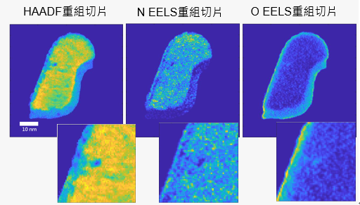
The 3D elemental distribution in advanced semiconductor components is critical to process inspection but has not achieved high resolution for a long time. This technology uses EELS combined with tomography to improve the resolution. The 3D determination of oxygen and nitrogen has achieved a resolution of 0.8 nanometers, the best record in the EELS tomography of semiconductor components in the literature. The tomography reconstructions of HAADF, EELS (nitrogen), and EELS (oxygen) were performed and then sliced at the same specific position, respectively. A void can be observed in those slices in the HAADF image, and the void size is estimated to be about 1.25 nm. This void can be observed in the 3D reconstruction of nitrogen and oxygen (the site in the nitrogen map is void, and that in the oxygen map is a bright spot). The TaN is not completely deposited, and there is oxide contamination.

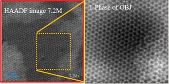
Due to the weak scattering of two-dimensional materials, it is difficult to identify their atomic structures in the STEM-HAADF image, and the size and the quality of the light source also limit the image resolution. Electron ptychography (4D-STEM) can overcome the resolution limitation caused by the light source. At the same time, because the phase is particularly sensitive to absorption, it helps to analyze light elements with a lower dose. The establishment of this platform will be a great benefit to materials scientists. The figure’s left is the STEM-HAADF image of a single-layer MoS2 2D material under a spherical aberration-corrected electron microscope. The accelerating voltage is 200kV, and the hexagonal arrangement can be roughly seen at a magnification of 7.2 M, but single atoms cannot be seen without image processing. The image on the right is the 4D-STEM reconstructed image under the same beam conditions. Each atom can be clearly observed, including point defects. After reconstruction, the image resolution can reach 0.8 angstroms.


