Å-scale characterizations in semiconductors encompass modern advances in instrumentations and material physics and call for dedications across disciplines. This project represents a concerted momentum toward the Å-scale characterizations through a harmonic synergy of four subprojects led by reputed electron and photon experts in Taiwan. Subproject 1 (Dr. Ming-Wen Chu) aims at developing high-speed atom-by-atom spectroscopy using scanning transmission electron microscopy. Subproject 2 (Dr. Chih-Wei Chang) intends for emergent instrumentations, measuring the crucial problems of heat dissipations in miniatured semiconductor devices and inventing new methodology for spatially-resolved elemental mapping. Subproject 3 (Prof. Shi-Wei Chu) pushes the limit of optical probing resolution both in axial and lateral dimensions. Subproject 4 (Dr. Yu-Ming Chang) boldly tackles deep-UV laser spectral microscopy technologies and their potential applications in semiconductor industry Indeed, the Å-scale characterizations in semiconductors concern how to go down to the very finite scale in space and, meanwhile, the knowledge required prompts for the fusion of cutting-edge knowledge across expertise. This project will not only shed light on the national endeavor of Å-scale characterizations in semiconductors, but paves the avenue to understanding semiconductors at Å scale by in-house developed instrumentations.
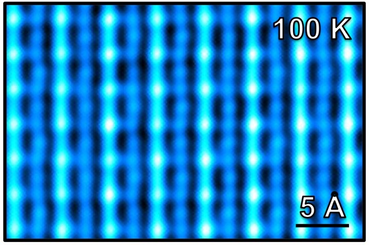
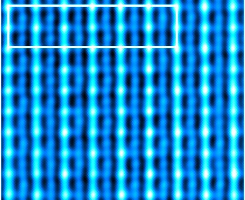
Fig. Cryogenic Scanning Transmission Electron Microscopy Imaging at 100 K (Rectangle, superlattice with 3 nm in width)


